Designing a fab-able minimal Arduino clone
I’m trying to design an Arduino-style board in the tradition of the Bueno board, but based on the simpler Arduino Uno (ATmega328p) architecture.
Source designs
There are many Arduino clones, some adopting a minimal approach. I’ve used some of these as the basis for this design. By analysing the documentation of these designs, I’ve been better able to understand what each component does, why it’s necessary, and whether I need it for my purposes.
Nick Gammon board
I used this as my primary source, not least due to the great documentation and schematics.
Gammon Forum : Electronics : Microprocessors : How to make an Arduino-compatible minimal board
Standalone Arduino
Arduino themselves have instructions for a breadboard version, with each component explained:
Arduino - Setting up an Arduino on a breadboard
Shrimp
Shrimping.it have a very simple breadboard version, but not much documentation. I have made this one myself.
This PDF is a good supplement, which gives some more detail: http://ve3rrd-shack.dyndns.org/files/makingtheshrimp.pdf
Most of what follows is based on the Gammon board. Where other designs differ, I’ve tried to understand what the implications of those differences are.
My objectives and design criteria
Use case
- A microcontroller board that can be produced in any fablab by novice students
- Produced using standard fablab processes: SMD components, hand-soldered, on a milled copper FR1 board
- Students should be able to take away a functioning microcontroller board which they can use in their own projects, which they have made themselves, rather than picked off the shelf
Objectives
- The board itself should be quick to mill and make efficient use of material
- Make board-stuffing a viable project for a soldering novice
- Reduce the likelihood of mistakes in milling, soldering or in use
- Make the finished board reliable, easy to program, and easy to use in projects
- The board should be safe, and not cause damage to other devices it’s connected to
Design criteria
- Use as few components as possible
- Use as small a board size as possible
- Expose all chip pins expected by the Arduino system
- Include standard programming interfaces
- Use minimal through hole components to reduce the need to hand-drill boards before stuffing
- Use SMD components of a size suitable for beginners - ie 1206s
- …
The board, step by step
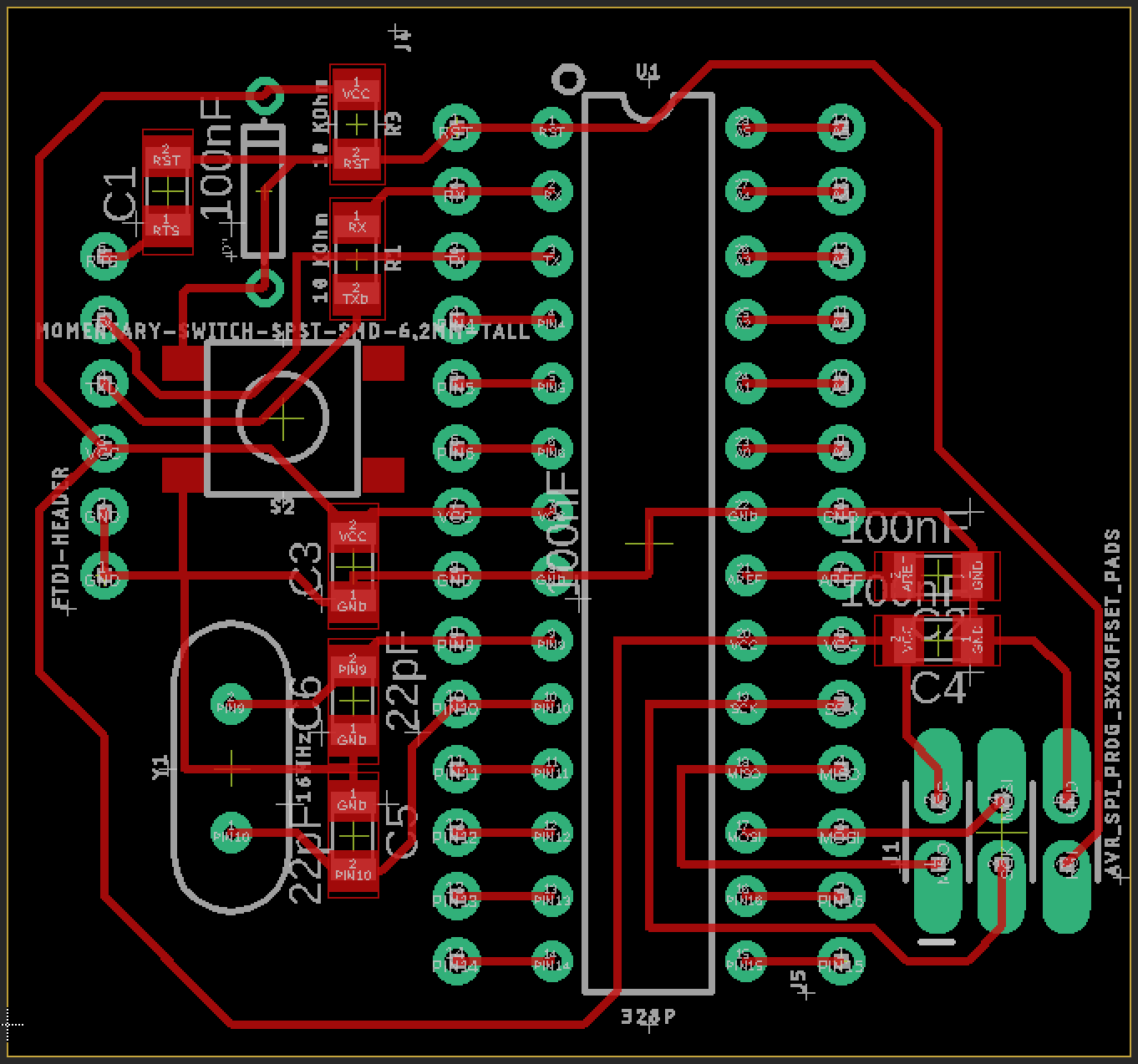
See a later post for discussion of this Eagle board layout. All the component labels below (e.g. “U1”) refer to this diagram.
Chip
- U1
Note orientation, also note care when handling. This should sit in a 2x14 pin DIP socket so the sockets can be easily soldered without risking the chip, and so that chip itself can be swapped out, or even programmed elsewhere.
Power
- Headers J4 and J5 (14 pin female header strips)
I’m just exposing the VCC and GND pins on these headers, to be connected up to whatever power supply is available. This is where a USB-compatible chip (like the 32u4) is nice. It’s easy to power it by the same cable and plug that you’re using to program it, and once it’s programmed, it’s easy to find a spare 5V USB power supply.
WIP - this could be improved.
There is no voltage regulator, nor is there any protection against multiple power supplies being connected at once. This follows the bare-bones approach used in Gammon’s board, and the Shrimp.
The very basics are to wire +5V to VCC and AVCC (AVCC is the analog power in), plus both GND pins (normal and analog).
…
There is no voltage regulator, that could be added without too much extra trouble. Without it you just hook it up to a 5V supply (probably 3 x 1.5 volt batteries would be fine).
Without a power regulator we need to take responsibility for providing a power supply of between 3V and 6V. This can be delivered by…
- A Lithium battery at ~3.7V
- Four NiCd or NiMh batteries at ~4.8V
- Three Alkaline batteries at ~4.5V
- a USB power supply at ~5V
… meaning you can choose the power supply suited to your project.
Since we avoid using a power regulation circuit, it is feasible to run a well-designed Shrimp project for several years off a small battery pack by using the ATmega’s low power modes, such as this sketch ; an example from our AlarmClock Project .
The standalone Arduino board uses a regulated supply. And according to this breakdown of the commercial Arduino Uno board, it has a few special power circuits:
There’s the power input from the 9V jack with voltage regulation. There’s the voltage management section, which prevents voltage from being sourced from USB and the 9V jack simultaneously.
…
PTC Resettable Fuses
There are a pair of resettable fuses on the schematic, but they have a semi-unusual symbol that you might not run into very often… sort of a box with a slash through it. Those are the cool little components that break the circuit whenever you inadvertently short circuit something and threaten to fry your computer over the USB cable.
Decoupling (aka bypass) capacitors
- Capacitor C3 (100nF) between pins 7/VCC and 8/GND
- Capacitor C4 (100nF) between pins 20/VCC and 22/GND
- Capacitor C2 (100nF) between pins 21/AREF and 22/GND (100nF = 0.1 uF)
Why have a bypass capacitor?
In a perfect world, 5V at your power supply ends up at 5V at your VCC pin on the chip. But because the traces and power supply and other components have internal resistance and inductance, when the chip is operating, the voltage at the pin can fluctuate, even falling below the operating voltage of the chip, which can cause the program to malfunction. Or the change in current can’t be serviced by the circuit (due to inductance) especially when the chip is switching at a high frequency. A bypass cap (which stores current) placed very close to the chip can provide the quick current needed for these high frequency changes, rather than getting the power from across the other side of the board.
Multiple caps (different capacitance values and different package sizes) give you low impedance across a wide range of frequencies.
See also What is a decoupling capacitor and how do I know if I need one? - Electrical Engineering Stack Exchange Also, this video on multiple parallel bypass caps with different values: EEVblog #859 - Bypass Capacitor Tutorial - YouTube

Also a good summary here: Decoupling capacitors
Bypass/Decoupling caps are needed due to the parasitic inductance and resistance inherent in wiring and PCB traces, inductance limits how fast current can change. When working with high frequency digital ICs, current must be able to change quickly. Adding the bypass/decoupling capacitors as close as possible to the IC’s V+ and GND pins effectively reduces the input impedance of the power supply + wiring.
You could also think of the bypass caps as tiny batteries that supply the IC with power until the power supply current can arrive to both fill the capacitor again and power the IC. The capacitor also passes any high frequency noise FROM the IC to ground, preventing interference.
Multiple value capacitors are used to cover multiple frequency requirements, or to have as low as possible ESR and ESL in the capacitance. MLCC (Mono/Ceramic) capacitors have extremely low ESR/ESL, but are also only mid capacity, they are the most common type of 0.1uF capacitors used for bypass. These are put in parallel with an electrolytic, which can filter the lower frequencies, but has higher ESR and ESL. When using an electrolytic, when the capacitors ESL/ESR is greater than that of the supplying circuit, their value cancels itself out in the best case, and they make things stop working in the worse case (see “capacitor plague”).
And on naming: Capacitors - learn.sparkfun.com
A lot of the capacitors you see in circuits, especially those featuring an integrated circuit , are decoupling. A decoupling capacitor’s job is to supress high-frequency noise in power supply signals. They take tiny voltage ripples, which could otherwise be harmful to delicate ICs, out of the voltage supply.
In a way, decoupling capacitors act as a very small, local power supply for ICs (almost like an uninterupptable power supply is to computers). If the power supply very temporarily drops its voltage (which is actually pretty common, especially when the circuit it’s powering is constantly switching its load requirements), a decoupling capacitor can briefly supply power at the correct voltage. This is why these capacitors are also called bypass caps; they can temporarily act as a power source, /bypassing/ the power supply.
Which ones do I really need?
Different DIY boards are more or less careful about the number of bypass caps needed. The breadboard Arduino has none (other than those on the power supply), the Gammon board had these three. The Shrimp has these, plus another 10uF between pins 20/AVCC and 22/GND.
Some rationale on this thread:Why use 2 decoupling capacitors?:
The 10uF capacitor, in conjunction with the supply leads, is acting as a line-load decoupling circuit. It keeps the power more even at the load point. They are generally not required where load currents are fairly constant, or where the power supply is very close to the load circuit and connected via a low impedance line.
And here: http://forum.arduino.cc/index.php?topic=120796.msg908955#msg908955:
Also where the caps are placed can have a big effect on how well bypass filtering work. The larger caps work better by placement at where power enters the board or right at the output of a voltage regulators, where as the smaller popular .1ufd caps are usually more effective mounted right at the Vcc terminals of any ICs being protected.
WIP I’ve left this one off for now, but it might be worth adding in a later revision.
Chip reset
- Resistor R3 (10 KOhm)
- Diode D2 (1N4148 signal diode)
- Switch S2
Usually used for uploading new programs to the chip. From the ATmega328p data sheet:
PC6/RESET
If the RSTDISBL Fuse is programmed, PC6 is used as an I/O pin. Note that the electrical characteristics of PC6 differ from those of the other pins of Port C.
If the RSTDISBL Fuse is unprogrammed, PC6 is used as a Reset input. A low level on this pin for longer than the minimum pulse length will generate a Reset, even if the clock is not running. The minimum pulse length is given in Table 29-11 on page 314. Shorter pulses are not ensured to generate a Reset.
The various special features of Port C are elaborated in ”Alternate Functions of Port C” on page 94.|
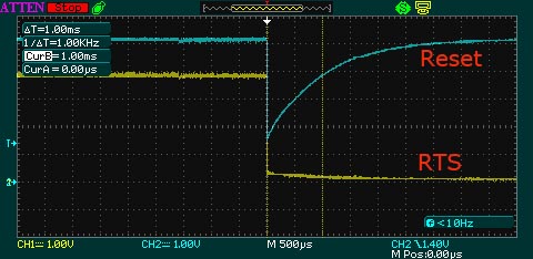
This pin should normally be held to 5V. You quickly pull this pin to GND when you want to reset the chip. According the table referenced, the minimum pulse width (time pulled to GND) is 2.5 micro-seconds. You can do it manually with the switch.
The 10 KOhm resistor between pin 1/RST and VCC holds this pin at 5V but stops current flowing. According to Gammon, the chip already has an internal pull-up resistor, but this external component “appears to make it reset more reliably when downloading new programs.”
He also adds the diode:
Without it the reset line may spike up to 10V when RTS goes high, potentially putting the chip into “high voltage programming” mode.
WIP In Gammon’s spec this is a 1N4148 signal diode. I’m not sure we have those in the lab, so need to check this…
See also the section below on programming, which makes use of the chip reset pin.
Timing crystal
- Crystal Y1 (16MHz) to pins 9/XTAL1 and 10/XTAL2
- Capacitor C5 (22pF) to pins 9/XTAL1 and 8/GND
- Capacitor C6 (22pF) to pins 10/XTAL2 and 8/GND
The 328p chip has an internal 8MHz clock, but can be run with an external timing crystal for higher speed and precision. We can use a 16MHz crystal, with two capacitors to reduce noise. These caps don’t have to be precise, eg. 18 pF or 20 pF will do. The external crystal is selected as the clock source by setting the appropriate fuses.
Clock Sources
The device has the following clock source options, selectable by Flash Fuse bits as shown below. The clock from the selected source is input to the AVR clock generator, and routed to the appropriate modules.
Table 9-1. Device Clocking Options Select
…
External Clock 0000
…
Note: 1. For all fuses “1” means unprogrammed while “0” means programmed.
WIP To simplify this board, you could use the internal clock - check the Lilypad for this, or this board: UDuino: Very Low Cost Arduino Compatible Development Board: 7 Steps (with Pictures).
Though note this could cause problems trying to program aa chip that has fuses set to expect an external clock: http://www.gammon.com.au/breadboard:
Chip not detected
Board Detector Output
Atmega chip detector.
This means that the target board has not entered programming mode.
First, double-check your wiring. If you are certain that is correct, then your target chip is probably configured to need a crystal. The crystal generates the processor clock, and without it you cannot program it.If you bought a “raw” chip direct from the manufacturer you should not have this problem, as the chips default to using an internal 8 MHz oscillator. But if you got your chip from a third party who already installed a bootloader, then the “fuse settings” may have been changed to expect the crystal.
ICSP Header (for programming the bootloader)
- AVR SPI Header J1 (3x2 male)
This 3x2 header is simply a convenient way of exposing the SPI pins on the chip for programming via a ISP ribbon cable with female 3x2 connectors.
| Header | Chip pin |
|---|---|
| MISO | 18/MISO |
| MOSI | 17/MOSI |
| SCK | 19/SCK |
| RST | 1/RST |
| VCC | 20/VCC (or any VCC circuit) |
| GND | 22/GND (or any GND circuit) |
FTDI Header
- Header “FTDI header” (6-pin female)
- Resistor R2 (10 KOhm)
- Capacitor C1 (100nF)
This is simply a convenient way of exposing the serial pins on the chip for programming via a 1x6 FTDI (or similar) cable.
| Header | Chip pin |
|---|---|
| GND | 8/GND (or any GND circuit) |
| CTS | not used/shorted to GND |
| VCC | 7/VCC (or any VCC circuit) |
| TXD | Via 10 KOhm Resistor to 2/RXD |
| RXD | 3/TXD |
| RTS | via C1 to 1/RST |
I’m still getting to grips with this whole system, and there are many areas that are confusing for beginners. This header does three things:
- Provides power (VCC and GND)
- Send and receives data (the program) (TXD and RXD)
- Controls flow of data between the programmer and the chip (CTS and RTS)
Before getting into each of these, let’s spell out some acronyms:
- CTS: Clear to Send
- RTS: Request To Send
- RST: Reset (don’t confuse it with RTS!)
- DTR: Data Terminal Ready
- FTDI: Future Technology Devices International - the makers of the most common programming chip
- Tx: Transmit (TXD: Transmit Asynchronous Data Output)
- Rx: Receive (RXD: Receiving Asynchronous Data Input)
- TTL: Transistor–transistor logic
- UART: Universal Asynchronous Receiver/Transmitter (a physical circuit to send/receive serial data)
1. Power: VCC and GND
This is pretty simple, but we might need to be careful that power isn’t also supplied at another point, e.g. on the ICSP header.
2. Sending and receiving data: RXD and TXD
TX to RX and RX to TX: In case you’re confused about why TX goes to RX and RX goes to TX (Unlike with SPI where MOSI goes to MOSI and MISO to MISO): http://www.gammon.com.au/breadboard:
Note that TxD on the FTDI cable goes to RxD on the chip, and vice-versa. This is because with serial comms one side transmits and the other side receives.
Unlike many of the similar boards, Gammon’s includes a 10 KOhn resistor between TXD on the FTDI header and RX on the chip. Some digging found this thread: SOLVED: FTDI to breadboard Arduino - not in sync error
Again I should add that I still don’t know WHY this worked, but I did notice that the FTDIfriend (FT232RL breakout board) sold at www.adafruit.com includes a 10k -pullup- series resistor on the TX line, yet the Sparkfun board does not; I’m not sure what that is there for. I followed the Sparkfun schematic in making my board (except I added a 0.1uf cap on the DTR line) -hence my issues-.
And this response (from Nick Gammon, as it happens): SOLVED: FTDI to breadboard Arduino - not in sync error
The series resistor you mentioned would have another purpose - to limit current to avoid damage to the chip(s).
Note that this thread also mentions pull up resistors on the TX and RX lines, which are not on Gammon’s board, but are on this schematic for an Arduino Nano.
3. Controlling flow of data, aka “Handshaking”: RTS and CTS
Different programmers use different pins to control the flow of data between programmer and chip. Gammon’s board assumes the use of an FTDI 232R USB to TTL serial UART converter cable.
RTS and RST: As with many of the pin naming acronyms, these seem like they are almost designed to confuse. RST on the chip pin is short for “Reset”. RTS on the FTDI header is short for “Request To Send”. It’s just a coincidence that these two pins with similar names are connected (via a capacitor). It’s not the same as connecting VCC on the FTDI header to VCC on the chip, where you are connecting like with like.
http://www.gammon.com.au/breadboard
The capacitor is there to turn the RTS signal into a pulse, so that when the computer brings RTS low, it briefly pulls reset low, and then the pull-up resistor charges the capacitor again, bringing reset high again.
(As noted above, the Gammon board uses an external 10 KOhm pull-up resistor here, even though the chip already has an internal pull-up resistor.)
The Gammon board doesn’t use the CTS pin on the FTDI header, this is just connected to GND.
RTS/CTS vs DSR/DTR handshaking
Some programmers use different pins to control signal flow. The FTDI FT232R chip supports at least two methods itself. For example, SparkFun sell a standard FTDI cable that uses RTS to send a reset pulse to the chip. But they also sell an FTDI breakout board that brings out the DTR pin instead:
https://www.sparkfun.com/products/9716
The major difference with this board is that it brings out the DTR pin as opposed to the RTS pin of the FTDI cable. The DTR pin allows an Arduino target to auto-reset when a new Sketch is downloaded. This is a really nice feature to have and allows a sketch to be downloaded without having to hit the reset button. This board will auto reset any Arduino board that has the reset pin brought out to a 6-pin connector.
This might cause compatibility problems: e.g. https://learn.sparkfun.com/tutorials/sparkfun-usb-to-serial-uart-boards-hookup-guide:
Note The signal difference on pin 6 may cause these devices to not be 100% compatible with devices designed for use with the FTDI TTL-232R cables.
It seems that Arduino themselves changed course, using RTS on earlier boards, then switching to DTR:
On the first board that Arduino developed that used an auto-reset feature the IDE used the RTS control signal to trigger the reset to the board. On later boards they changed to using the DTR signal to use that (I recall no reason given for the change) for the trigger signal. So to keep compatibility they had to issue both RTS and DTR pulses. There should be no issue in the future but who knows what the future may bring. One issue is that when opening the serial monitor the DTR is pulsed which causes a board reset and I don’t recall if opening the serial monitor pulses RTS or not, probably not and it would be easy for you to test this.
I have an eBay FTDI programmer, and a Shrimp CP2102 USB to UART programmer (which seems to be a clone of the FTDI chip). Both of these bring the DTR pin out to the header, although on both the RTS pin is also accessible. My hunch is that DTR is the more ‘modern’ way of reseting the chip and what I should work on for now.
WIP: Verify that I can program the board using programmers that expose the DTR pin instead of RTS
Things to add/change
I’m going to leave this board as-is for now, and try to design one in Eagle that includes all the systems. However, there are already some things I’d like to address.
Power headers and control
The only way I can get power to the board is by connecting VCC and GND pins to a 5V power source. Same for powering a component, such as a motor, from the board. This isn’t the best approach. Note e.g. https://learn.sparkfun.com/tutorials/sparkfun-usb-to-serial-uart-boards-hookup-guide
Warning: These boards are for prototyping ONLY. Unlike commercial devices, power negotiation and suspend mode do not occur, and it is possible to overload the USB host. Exercise caution when connecting a load, and /never connect a load that draws too much current.
Adding a Blink LED
Pin 19 on the ATmega328 is “SCK/PCINT5 – Port B, Bit 5”. In the Arduino IDE, this is also known as digital pin 13, and often used to flash an LED in a Blink sketch. On the Uno, there is an LED connected to this pin on the board itself.
This would be a nice thing to have on the board. It would also need a current-limiting resistor (100 Ohm)
Next steps
I designed a board along these lines in Eagle to see how all these ideas work within the physical constraints of a board layout. That is documented separately.
I don’t currently have access to a lab to fabricate a test board, but that is also on the list.
I’d also like to do an alternate version that is as simple as possible, while still being usable.