Designing a v0.1 board in Eagle
A first draft at a board layout for the fab-able Arduino.
I have covered the design process for this board already. IBut I wanted to try creating a schematic in Eagle, and laying out a board to see how it works in practice
Files on Github: /board-designs/diy-arduino-0.1
This design is as far as I can really go without attempting to mill and test it.
I can already see some problems:
Size
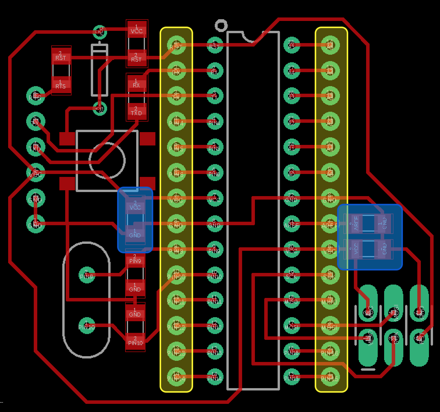
This board is about 9cm in each dimension. The smaller FR1 boards we have in the lab are about 8 x 15cm, so it could probably be squeezed down to fit, but it’s still too big. If we want to mill several at once, and do it quickly, I need to make the overall size smaller.
14 pin headers (highlighted in yellow)
I added these two 14-pin headers to access all the pins on the chip.
It’s a simple solution, but has a few downsides:
- Adds to the size
- These are female headers, which have through-hole pins underneath. That would mean drilling (or maybe milling) 28 holes for these pins. Very time-consuming
- The simplest place to locate them is inline with the chip, but this pushes the decoupling capacitors (highlighted in blue) away from the chip. Really they should be as close as possible.
Tried to make it as compact as possible, but this is still about 8 x 9cm, which would take a long time to mill, so it would be good to get this down:
Lots of headers
I have those two headers to access the I/O pins, plus the ICSP header and the FTDI header. These are convenient, but perhaps overkill. Maybe I could get rid of the FTDI and ISCSP headers and just use loose wires to connect to them when programming. Some labelling of pins on the board might be enough to make this easier.