Guide: Drawing a circuit in Eagle
Workflow and tips for drawing circuits in Eagle
Libraries
- Part: e.g. a 10k resistor
- Package: surface mount or through hole, size, etc.
- Specs: current it can handle, accuracy, etc.
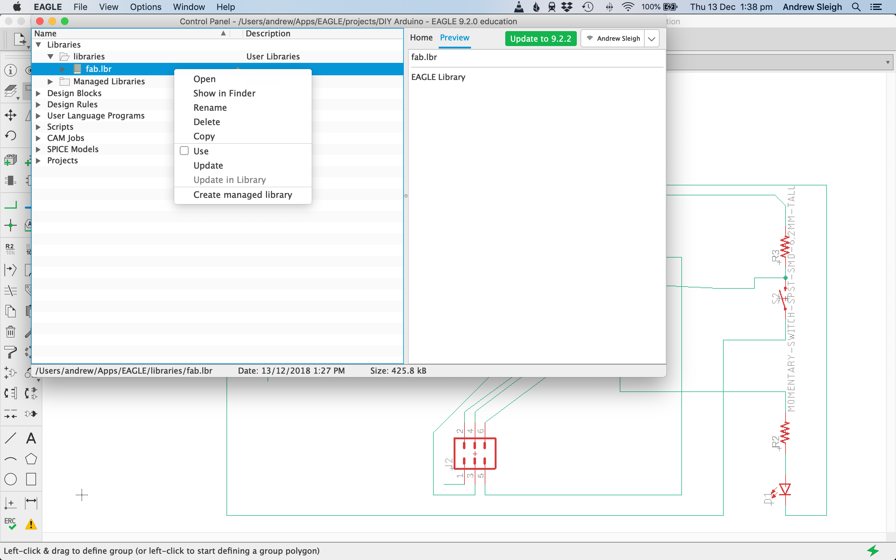
There is an Eagle library of standard parts from the Fablab inventory
- Download: https://gitlab.cba.mit.edu/pub/libraries/blob/master/eagle/fab.lbr
- Make sure it’s named
fab.lbr - Move to your Eagle Library location. Something like:
/Users/YourName/Documents/EAGLE/libraries/ - Open the Eagle Control Panel (under
Windowmenu) - Find library you added, right click and select
Use
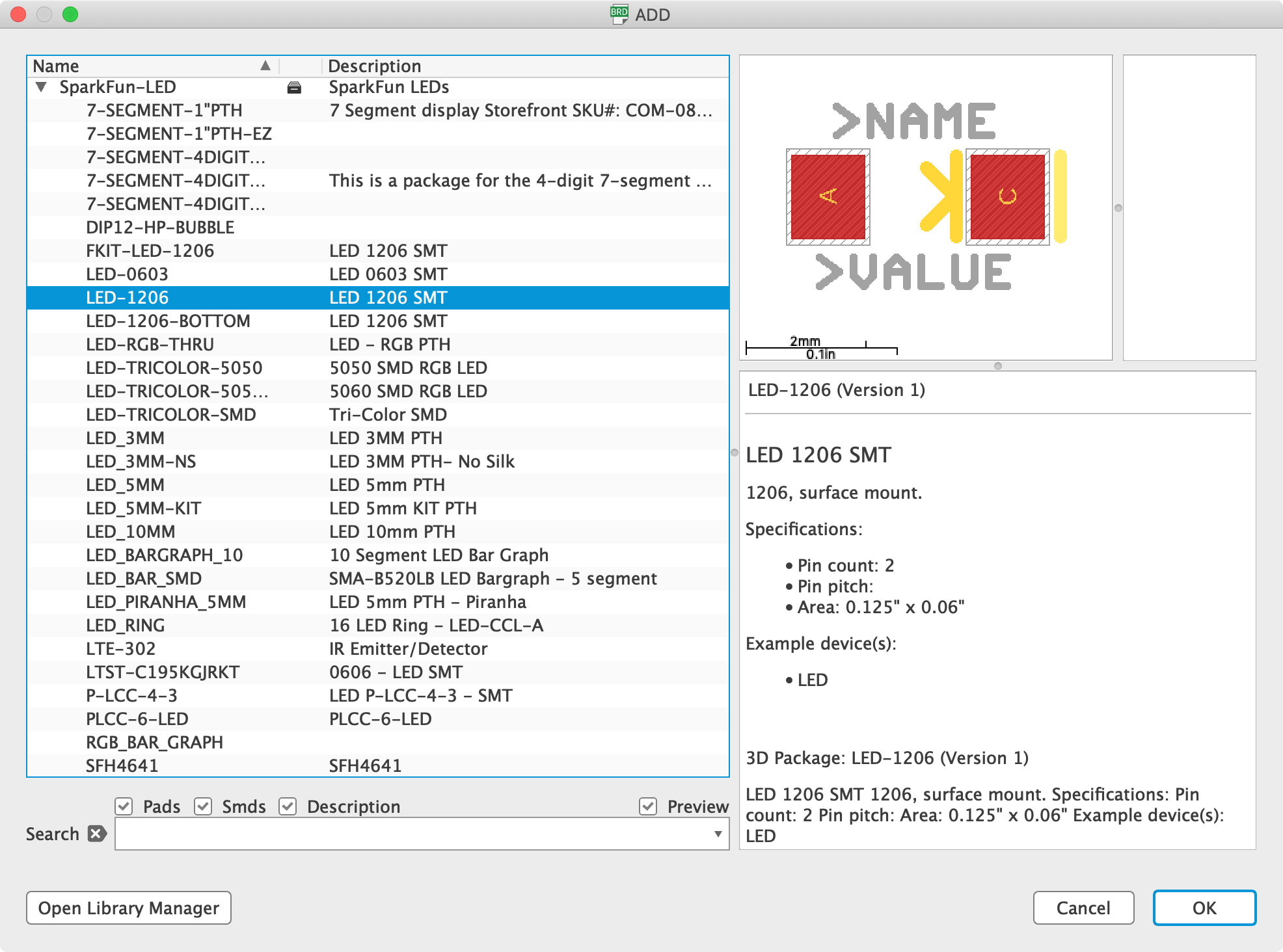
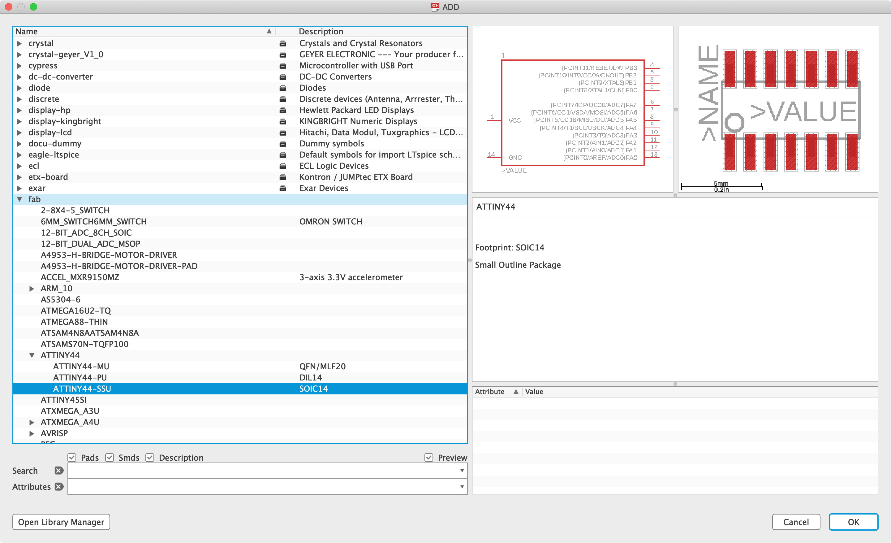
Open a schematic, add a part (which opens the Library window), and you should be able to select parts from the fab library:
Schematic
Logical structure of a circuit.
How are the components connected.
Abstract, not a visual representation.
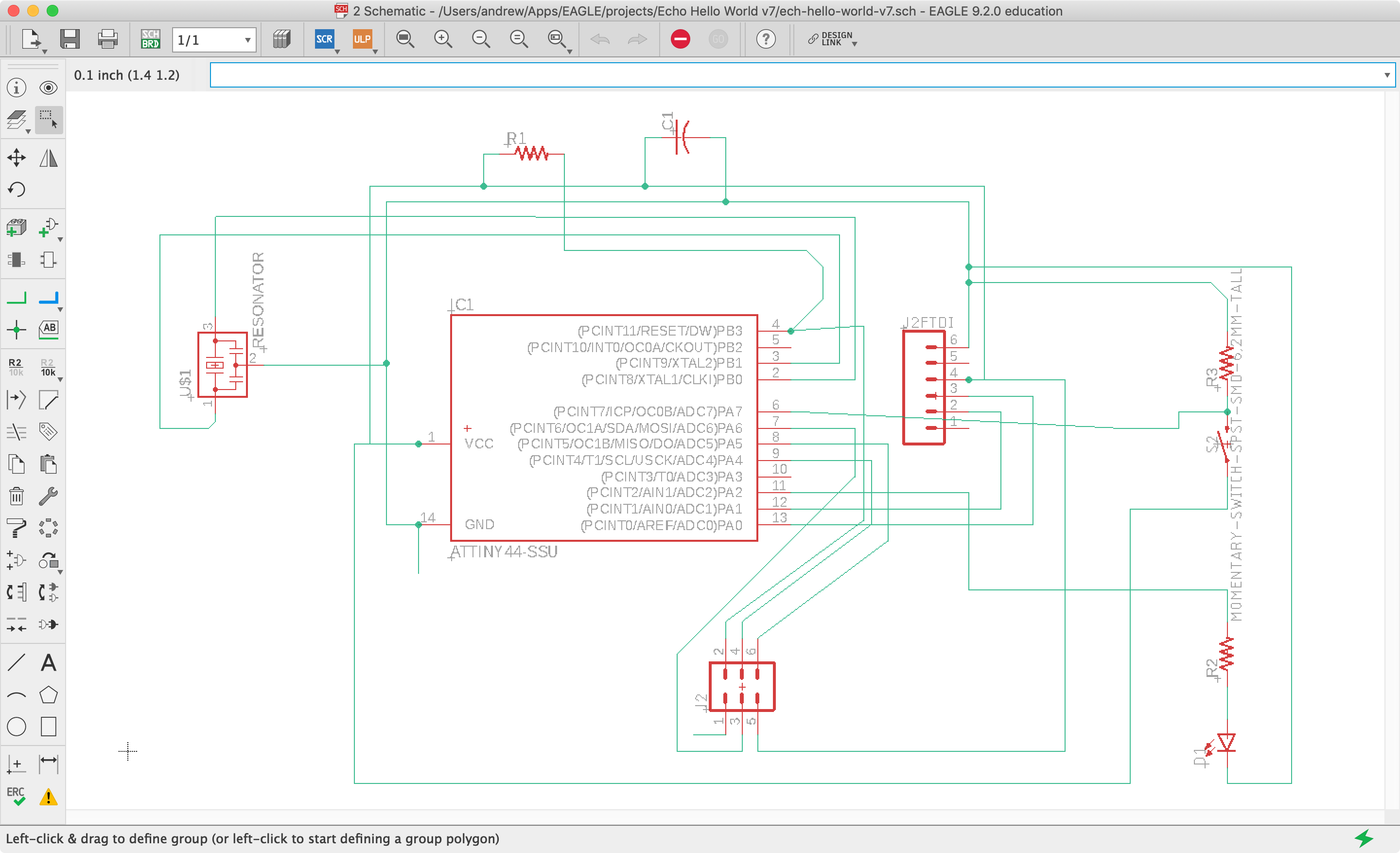
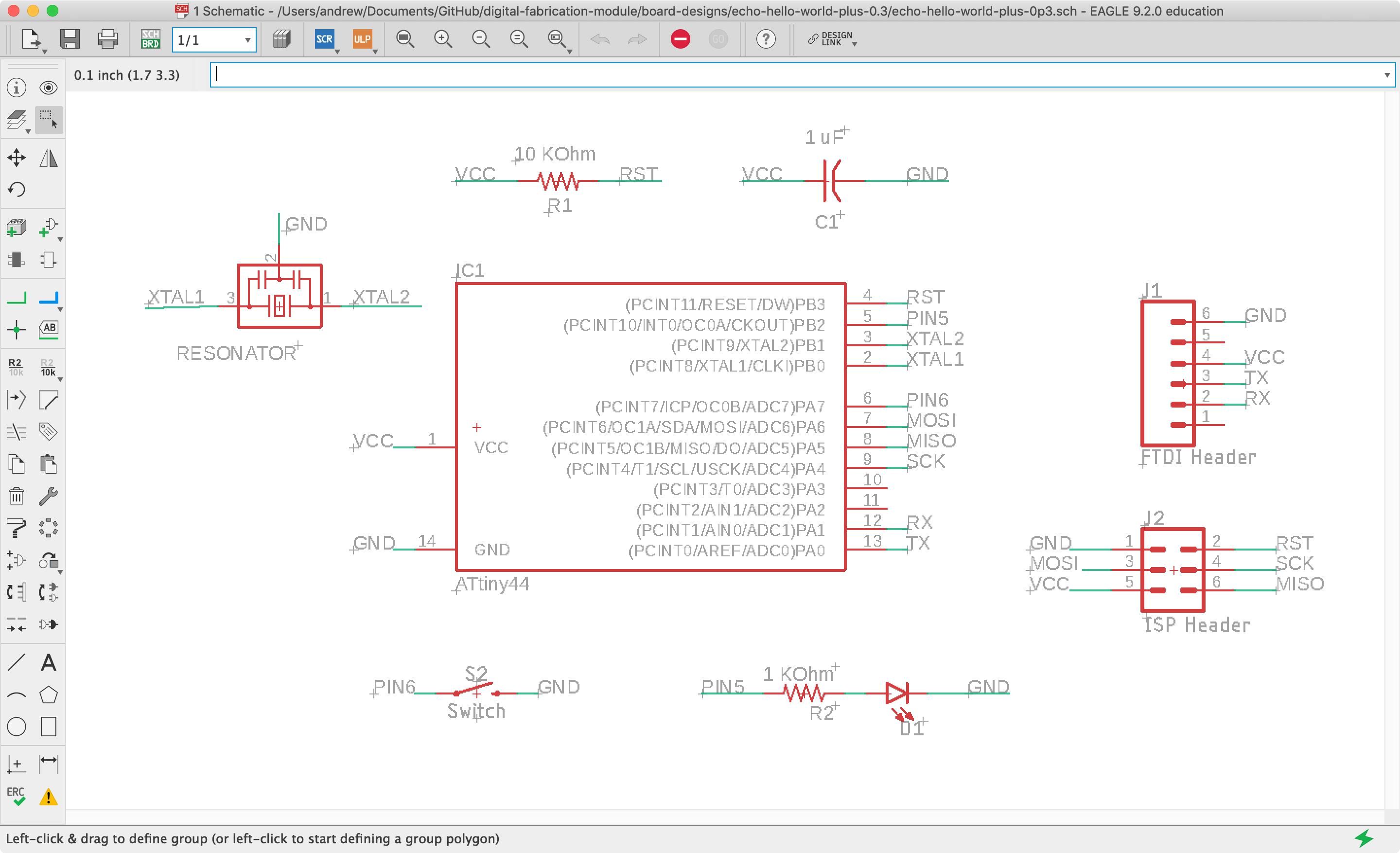
My schematic for Hello World board.
Green lines show connections between parts.
Parts are in red - notice chip doesn’t look like that.
Once you’ve got used to Eagle, its easier to connect points by names instead of lines.
Board layout
This is a visual representation of your board.
Where the components go on the board, and how to route traces (connections between parts) between them.
How to satisfy the requirements of the schematic, within the constraints of the fab process (aka design rules). Mainly: how thin can traces be, how close together can they be.
Layers: we’ll only make single layer boards.
Use SCH/BRD button on toolbar to switch between Schematic and Board layout views.
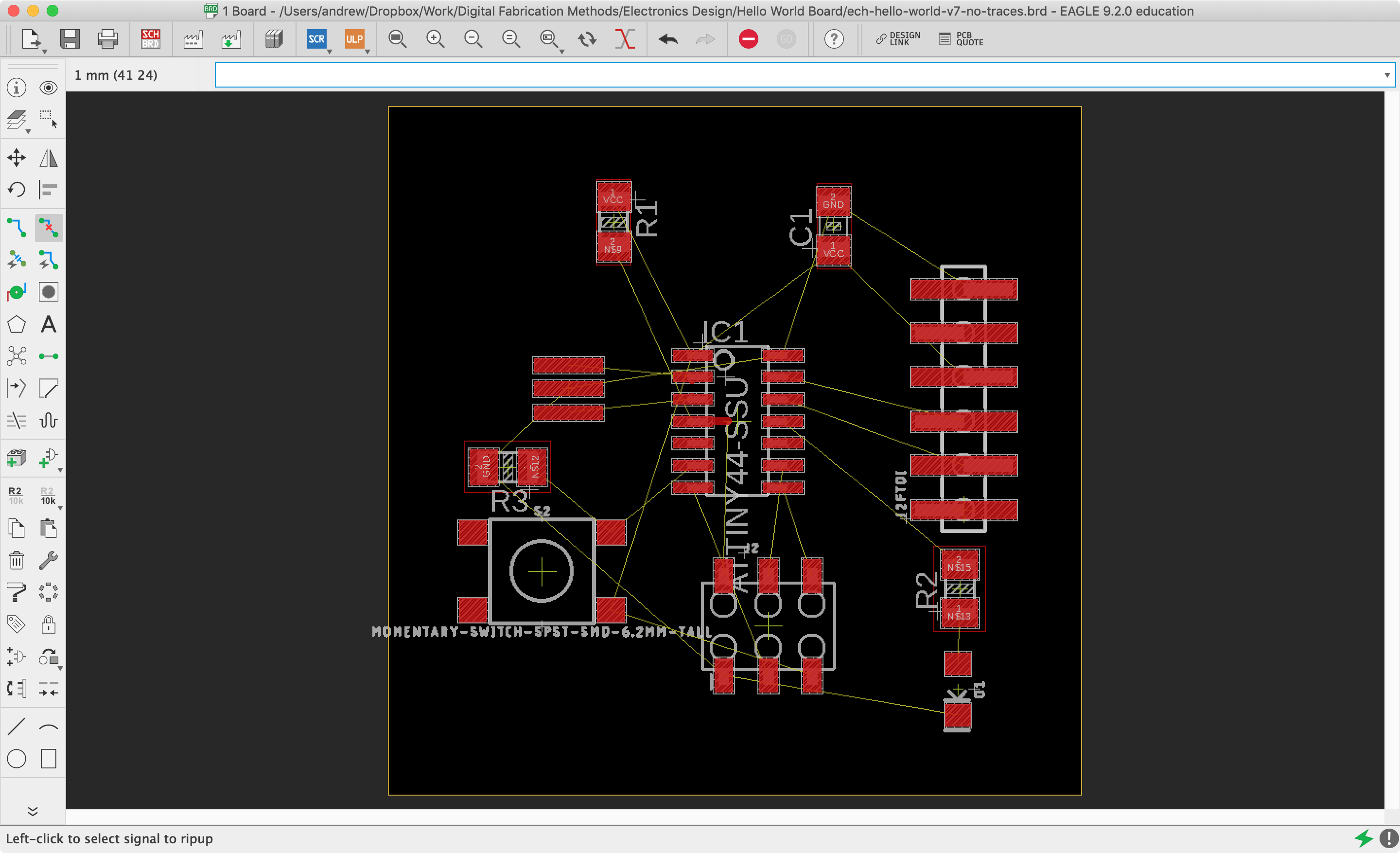
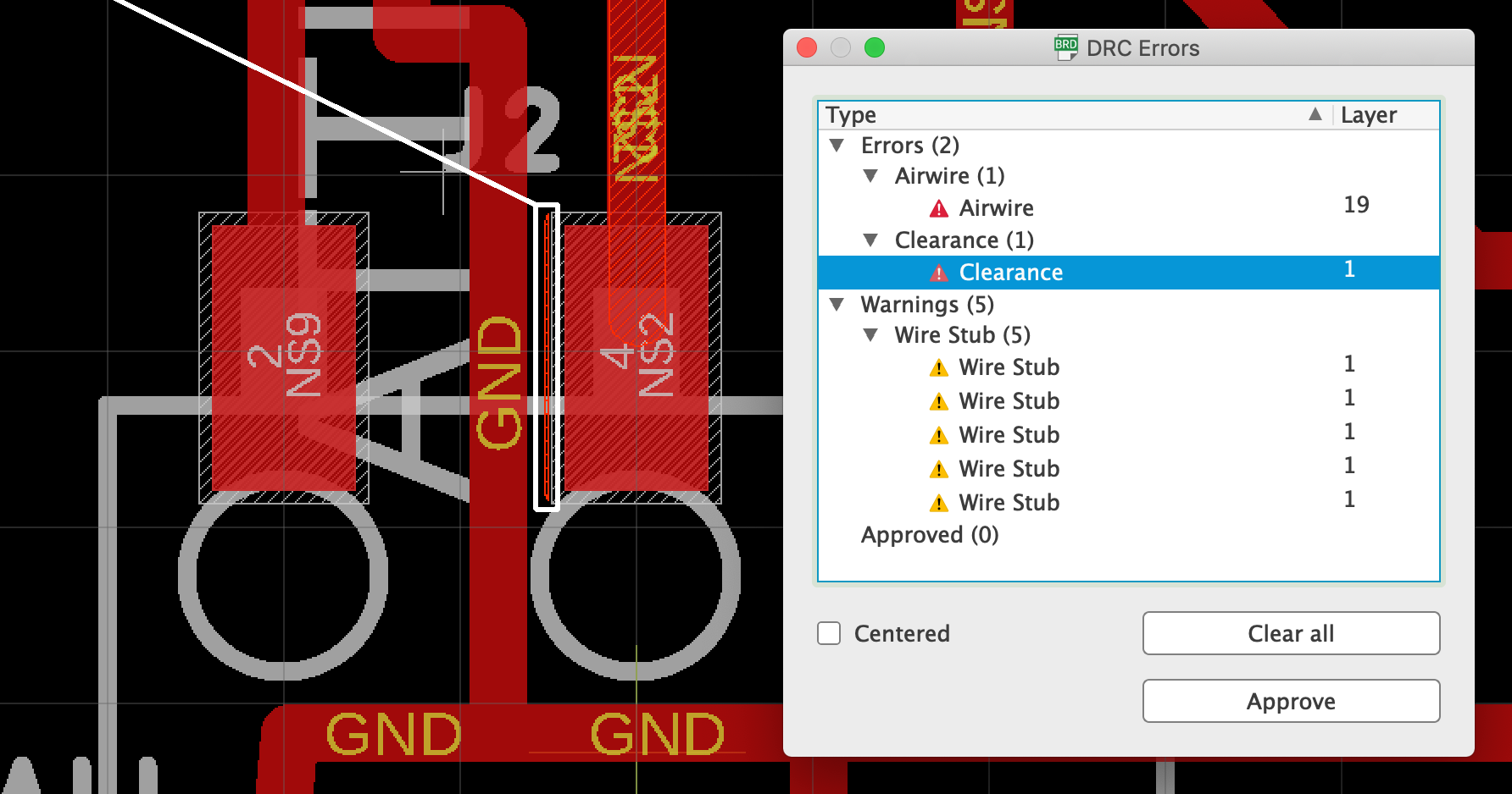
Yellow lines are “Airwires”.
Your job here is to convert the airwires into traces.
Tools are frustrating at first. Eventually satisfying, like solving a puzzle.
Art: place parts well, process of trying placement and routing, ripping it up, try again.
Tricks: rotating parts, or running traces underneath.
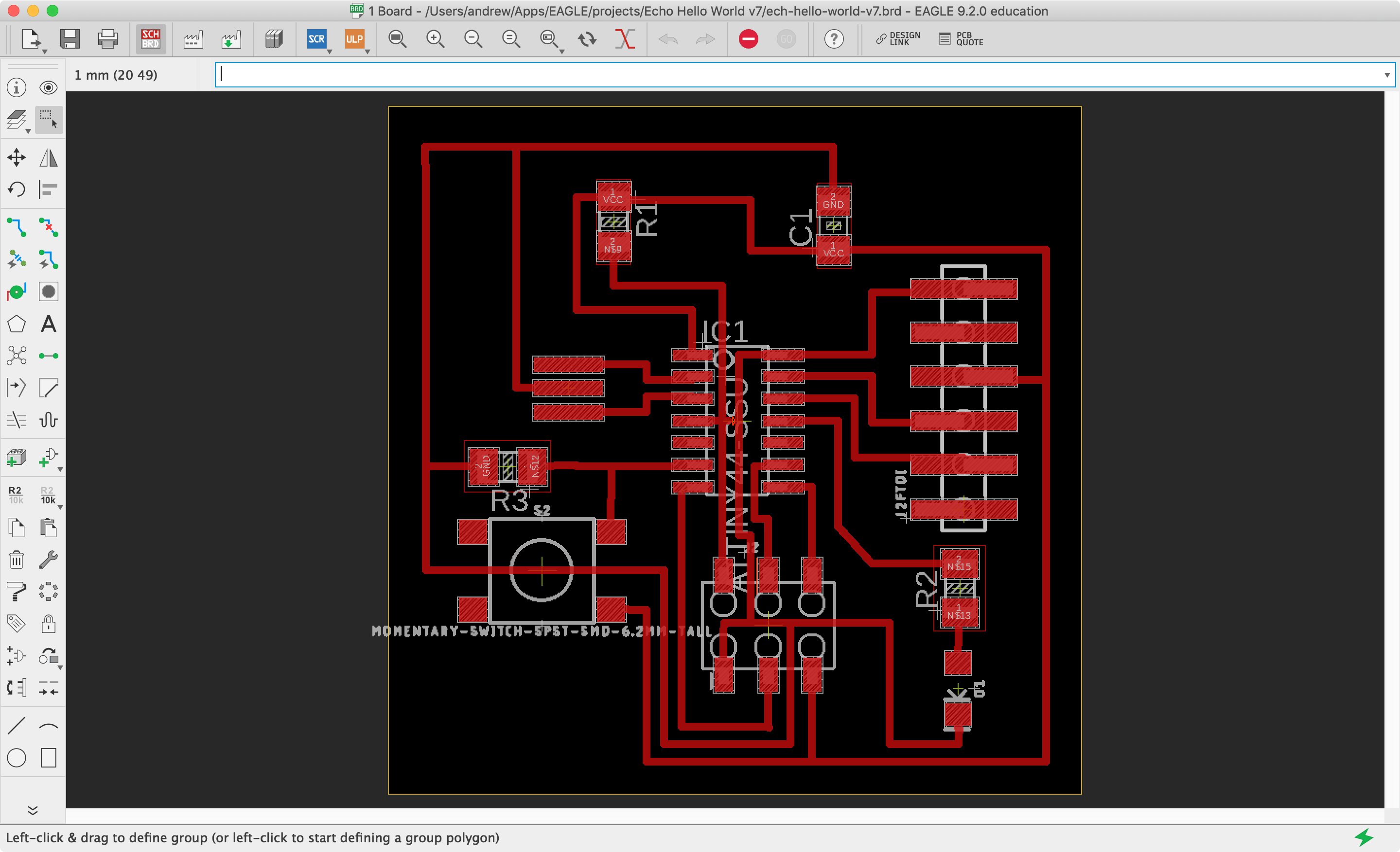
Red lines are traces.
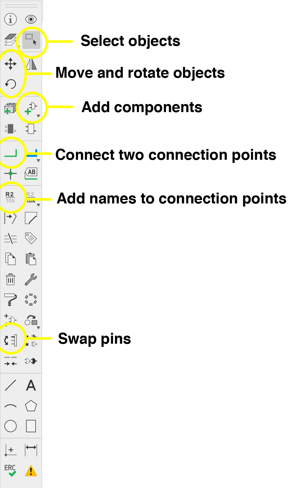
Common tools:
| Schematic | Board |
|---|---|
 |
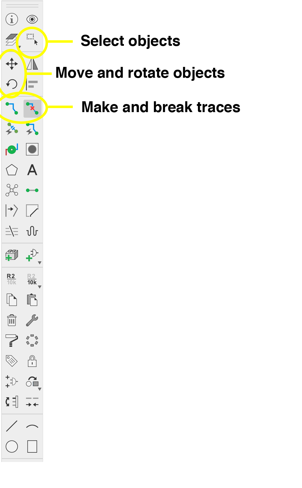 |
Units and grids
View menu > Grid…
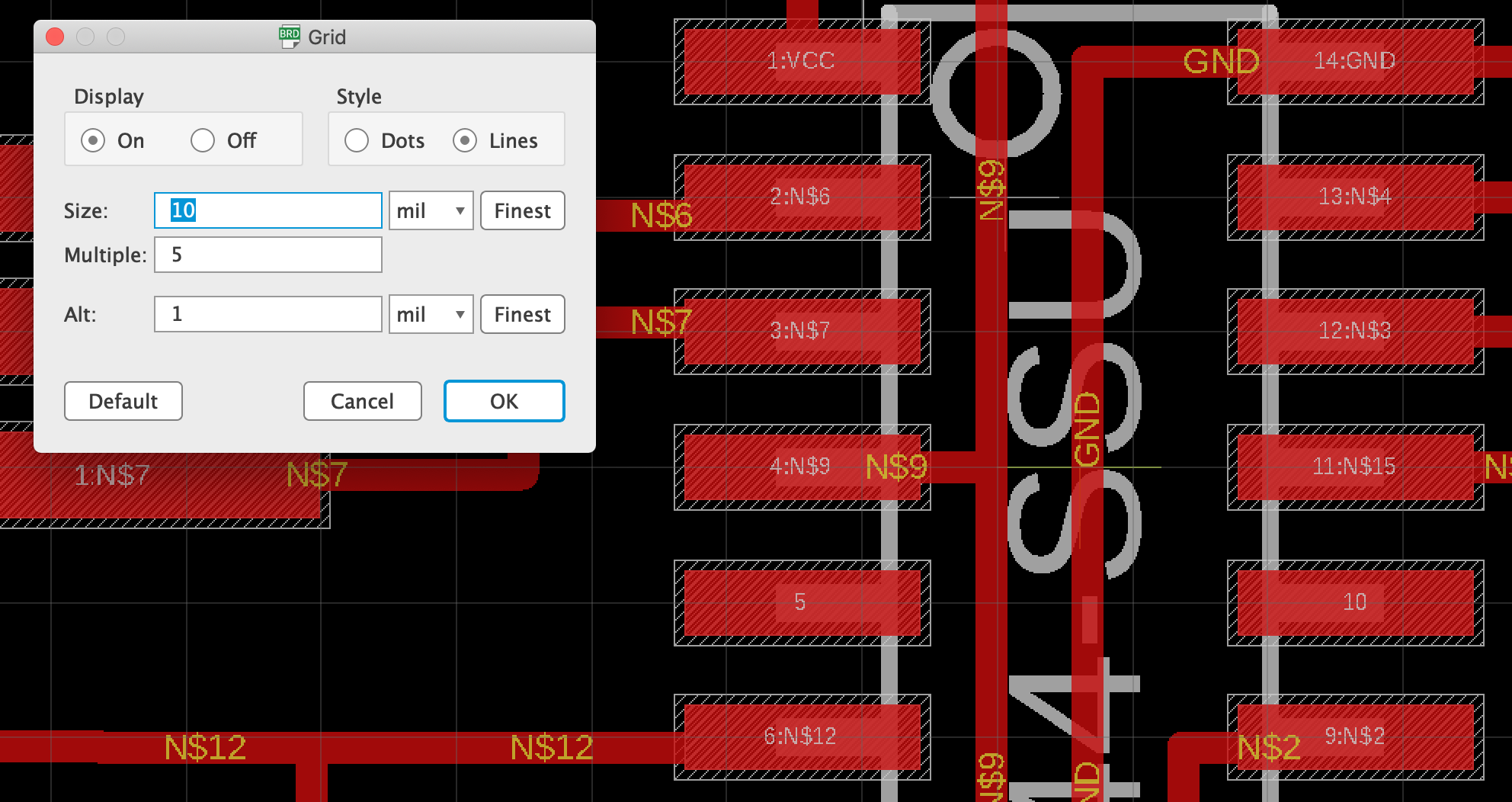
Beware: ‘mils’ != ‘mm’
A ‘mil’ is 1/1000 of an inch.
A standard pitch (ie the distance between the center of two holes or pins on a component) is a multiple of 1/10 of an inch (0.1”), or 100 mils, or 2.54 mm. So it can be useful to stick to ‘mils’ as a unit of measurement when laying out boards.
Other tools you might Use
DRC: Design rules
Tools menu > DRC…
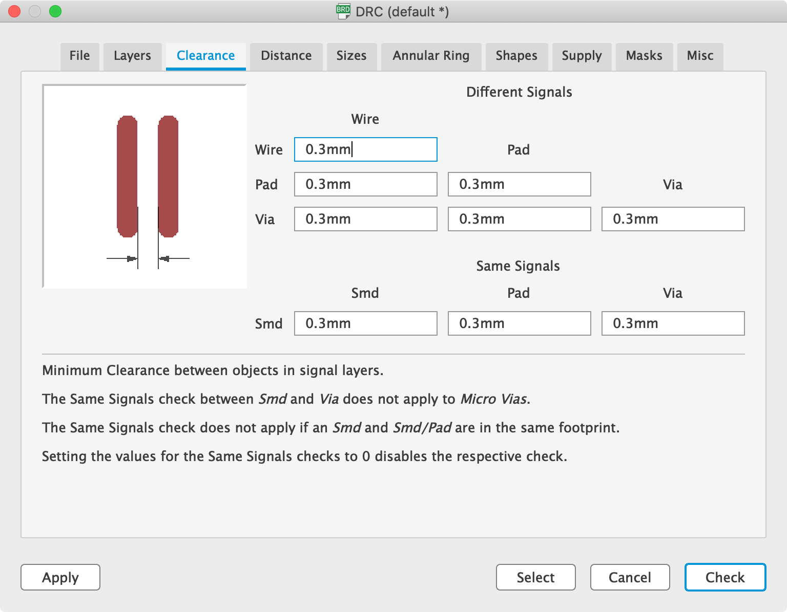
Lets you check for clearances between pads and traces. If our milling bit is 0.3mm, we need at least this much space beween all traces.
Adjust for different bit sizes.
You can fix some of these problems after exporting a PNG in an image editor - e.g. make a pad a little smaller (but don’t change the pitch of pads)
ULP (User Language Programs): Change all trace widths
Allows you to set all your traces to one size, all at once.
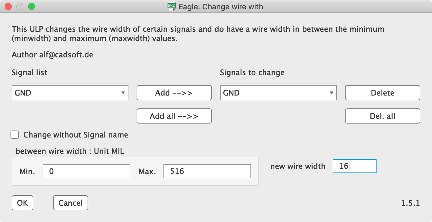
Toolbar: ULP button
Select cmd-change-brd-width from the list
“This ULP changes the wire width of certain signals and do have a wire width in between the minimum (minwidth) and maximum (maxwidth) values.”
Press Signal list : Add all -->>
Set new wire width to whatever wire width you need.
Bear in mind units: 1 mil = 0.0254 mm.
12-16 mil is not a bad trace width range (0.3 - 0.4 mm)
Prepare artwork for milling
Once circuit is complete, adjust board boundaries to be as tight to the edges of the circuit as possible - leave a few mm gap.
Many ways to turn your board layout into a millable design:
- I recommend: export layered DXF file from Eagle, edit in vector or bitmap application, generate hi-res PNGs for traces and board outline
- Switch un-needed layers off in Eagle, export hi-res PNG. Create outline separately.
- Print PDF file from Eagle. Edit externally.
- Use Eagle’s CAM Processor. Edit externally.
Export circuit layout from Eagle
I recommend exporting layered DXF file, then editing in Illustrator or Photoshop.
Import into external editor
When importing into an image editor, make sure you keep units and size the same.
Make adjustments
Delete or hide all layers you don’t need. Leave only pads and traces visible.
Make all your traces and pads white, and everything else black. (black material is milled away).
Make any adjustments for clearances.
Add any vector art or labels.
Create an outline mask
Create a white canvas, with a black line around the outside. The traces should fit comfortably inside this black line.
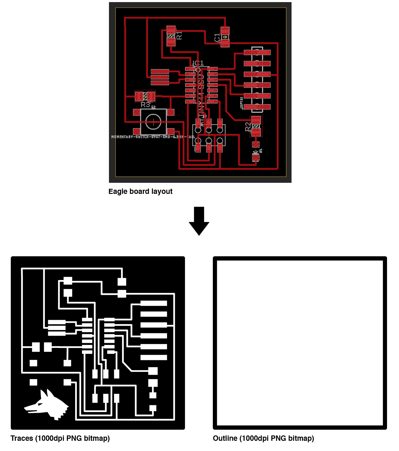
Important: Your traces PNG and your outline PNG must be the same size.
When you mill your board, you use this outline PNG to create a separate tool path to cut the board out from the copper sheet.
Export PNG images for traces and outline
- PNG: Uncompressed format, i.e. no artefacts
- Very high resolution: 1000dpi, because we’re machining at a resolution of 1/1000 of an inch
- Back and white (1bit)
- Editable - creatively, or to fix milling problems
5. Verify
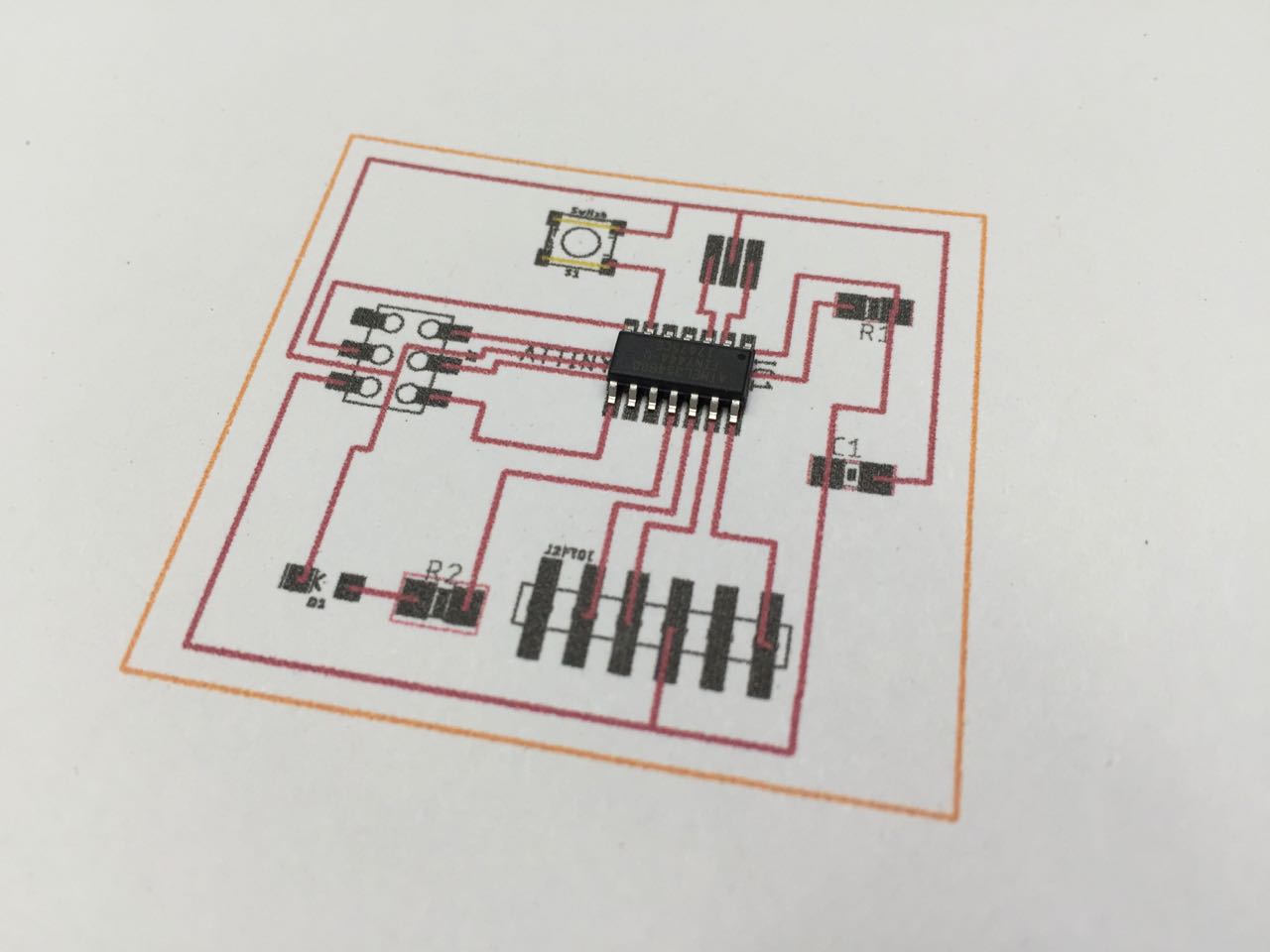
Print out your PNG at 100% and place some components on the printout. Do they fit? Are there overhangs that interfere, or bits you need to access that you can’t reach (e.g. a USB or power socket)?
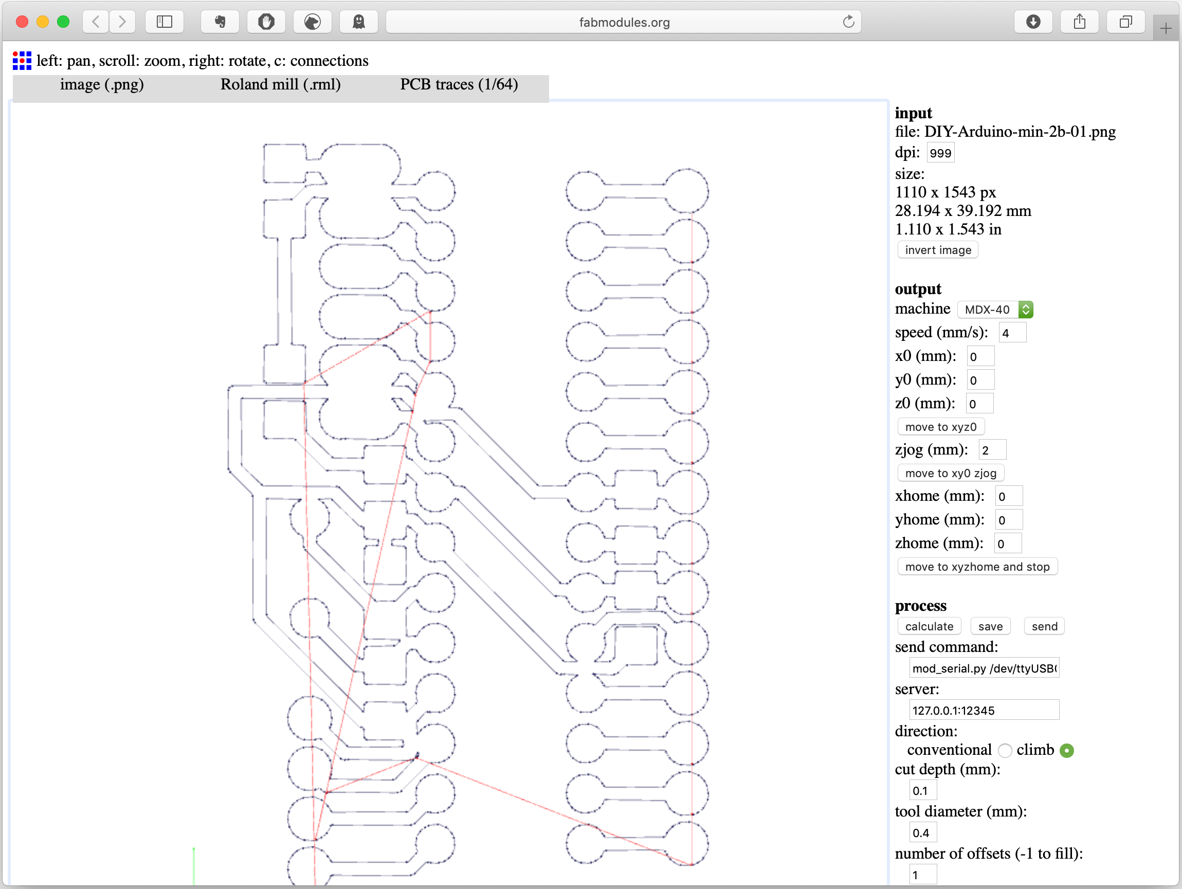
Try generating a tool path in Fab Modules. Is there enough clearance between traces/pads?
6. Testing a finished board
- Multimeter - check for continuity or shorts.
- Oscilloscope - measure voltage over time, see what signals pins are sending.
- Try to program.
Further reading
Eagle manual - installed with Eagle.
Sparkfun Eagle tutorials